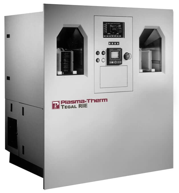
Plasma-Therm® now offers the Tegal™ Diode Reactive Ion Etching (RIE) systems. The Tegal Diode RIE systems are industry-leading systems for non-critical etching of dielectrics and photoresist trimming operations.
Non-critical dielectric etching equipment is especially useful for shifting machine load away from critical etching operations, meaning equipment running critical etching operations can run longer between routine maintenance. This improves the overall throughput of the facility.
Photoresist trimming operations can also improve the throughput of the facility by reducing the dimensions of photoresist beyond that achievable by lithography alone. This means smaller features can be created reliably, meaning higher yield and less time spent in rework.
What are the capabilities of each Tegal etch system?
Tegal 901ACS and 903ACS
The Tegal 901ACS and 903ACS systems are well-suited for semiconductor processing of silicon, but also for gallium-arsenide (Ga-As), indium-phosphide (In-P) and silicon-germanium (Si-Ge) substrates. They can plasma etch a variety of materials, including silicon dioxide, silicon nitride, and silicon carbide. They are versatile, capable of handling 75 mm, 100 mm, 125 mm, and 150 mm diameter wafers, as well as 4-inch square wafers, including thinned, insulating and transparent materials. Features down to 1 micron can be etched using these systems.
The 901ACS is a wide-gap diode reactor system. It is particularly suited for low-temperature plasma etch operations, geared towards etching delicate materials, such as organics and easily-damaged coatings and devices, without the use of clamps or electrostatic mechanisms for wafer manipulation. The 903ACS is a narrow gap diode reactor system, making it ideal for tightly-controlled, anisotropic etching of silicon dioxide and silicon nitride insulating layers.
Tegal 981ACS
The Tegal 981ACS is a scaled-up version of the 901ACS, specifically built to handle 150 mm and 200 mm diameter wafers, as well as 100 mm square wafers and 6-inch square wafers for non-critical photoresist removal, photoresist trimming, and large-scale etching operations. The 981ACS can be used for planarization operations and backside etching, all of which require etching over a very large area.
The Tegal 981ACS is similar to the 901ACS, but with some expanded capabilities. It has all of the same familiar features: a small footprint, an intuitive, touchscreen interface, and long-lasting, low maintenance parts. The 981ACS is also commonly used for BioChip nanotechnology applications.
Tegal 6500 HRe- Dual Frequency Etch System Series
The Tegal 6500 HRe- Dual Frequency Etch System hosts a cluster of plasma etching tools, which can be configured with one or two etching chambers. All 6500 series systems can be programmed to perform serial or parallel wafer processing from single or dual loading ports, depending on the configuration and application. This system uses dual-frequencies for high-density, capacitively coupled plasma (CCP) generation and magnetic plasma confinement. All of this allows for very precise plasma control, meaning etching can be performed down to the sub-micron level.
Tegal 6500 series etching systems are available in several varieties. The 6510 is capable of performing gate etching operations in polysilicon, as well as shallow trench isolation (STI) operations. Designed for precise etching, it can etch features as small as 90 nm on nitride and oxide hard masks.
The Tegal 6520 can perform etching of aluminum alloys down to the sub-micron level. This system comes standard with a rinse-strip-rinse (RSR) procedure, which removes contamination due to corrosion that can be left behind during etching operations of aluminum or steel. Because of RSR, the 6520 is especially useful for etching aluminum alloy interconnects and metallization layers, as it can anisotropically etch thick layers (> 2 microns).
The Tegal 6540 is designed for etching high dielectric coefficient materials (high-K), often used in capacitors, platinum and iridium electrodes, gold interconnects, and other difficult-to-etch materials. This includes lead-zirconate-titanate (PZT), strontium-bismuth-tantalate (SBT), and barium-strontium-titanate (BST), which are often difficult to etch. Features as small as 90 nm can be etched with this system, making it popular amongst manufacturers who produce high-density, high capacity DRAM and embedded memory devices, as well as non-volatile Ferroelectric Random Access Memory (FeRAM) devices.
What are the benefits of Tegal diode etch systems?
The Tegal series etch systems offer a small footprint on the factory floor, freeing up space for other equipment and maintenance tasks. The 901ACS, 903ACS, and 981ACS have no external rack-mount electronics, and the 6500 series only has one rack-mounted device.
In terms of maintenance, these systems are easily maintained, with low-cost, yet long-lasting consumables and a minimal operating cost. The long-lasting components mean increased uptime and higher system throughput.
Built-in data logging and archiving capability, standard SEMI Equipment Communication Standard (SECS) and Generic Equipment Model (GEM) hardware support, and an intuitive graphical user interface (GUI) make operations easy to monitor, maintain and troubleshoot.
All Tegal Diode RIE systems handle wafers cassette to cassette, meaning there is no manual wafer handling. This minimizes contamination, static discharge, and mechanical shock during wafer movement, increasing overall die yield.
Also, all electrodes are precisely temperature controlled. This reduces wafer-to-wafer variation, increasing yield and decreasing the time spent in reworking operations, and decreasing the scrap volume.
Final Word
The Tegal Diode RIE systems are a way to boost production by reducing load on critical etching equipment. They can handle large wafer etching operations, such as backside etching and planarization, but can also handle finer etching details down to 1 micron. The low cost of operation and small footprint make them suitable for virtually any semiconductor fabrication facility.
The Tegal Diode RIE systems are only available through Plasma-Therm. To learn more, contact Plasma-Therm today.

